Today's plasma etch technologies can be largely divided into two categories: reactive ion etch (RIE) and high density plasma(HDP). RIE is based on parallel plate discharge technique and used more for physical etching which needs energetic ions. HDP uses plasmas with many orders higher densities and works in the mTorr range hundred to thousands times lower than RIE. HDP technology is more favored for chemical etching of small
features.
Both technologies were developed primarily for silicon semiconductor manufacturing. It is hard to tell which technology is better for non-silicon materials which are being used in many electronic devices.
The HiEtch Processing System is using BMR's patented, proprietary Inductive Coupled Plasma(ICP) technology. HiEtch provides wide process windows covering HDP technology and many RIE processes, making process development of various new thin film materials substantially easier .
― Vertical position of the chuck can be adjusted to obtain
optimum process result
― Helium back side cooling
― Uniform coupling of RF bias power
Uniform Gas Flow
― Proprietary shower head gas injection
― Uniform pumping
HiEtch's wide array of process windows enables etching of various new thin films materials:
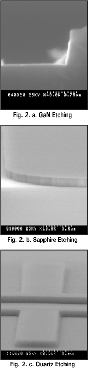
LED Materials - GaN, Sapphire
Compound Semiconductor - GaAs, InP
Ferroelectric Materials - Pt, PZT
Ceramic - Al2O3 , ceramics
Quartz
HiEtch's wide process window makes it ideal for initial development of new processes. Also, the inherent modular design makes the transitions easy from initial process development stage to pilot production and on to mass production.
The capability of depositing dielectric films at substantially low temperature with excellent quality opens a new application of plasma CVD films, including a wide array of microelectronic devices :
Precise Pressure Control: 1mT ~ 100mT
Source RF Power: 13.56MHz up to
2.5 KW
Bias RF Power: 13.56MHz up to 1.25 KW
Controllable DC Bias
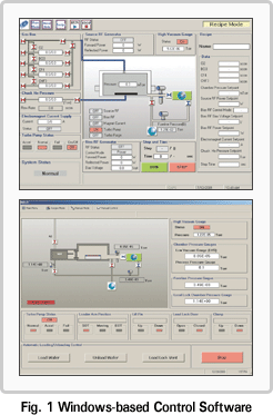
Windows-based Control Software
Magnetically levitated TMP
Heated Chamber Wall
Heated Foreline
Al 6061-T6 Hard Anodized Chamber Wall
Movable Chuck with 10cm travel
Helium backside cooling (ESC optional)
Automatic Loadlock
Up to one 200/150mm, two 100/75mm, Six 50mm wafers
High Density Plasma (HDP) etching technology was originally developed for silicon semiconductor industry to etch small size features. Many HDP techniques have been developed, and can be largely separated into two categories: resonance plasma (RP) source and inductively coupled plasma (ICP) source. Resonance type plasma sources include helicon, helical resonator, electron-cyclotron-resonance (ECR) plasma technologies.
The process windows for resonance plasma type sources are very narrow since they have to meet resonance conditions. Subsequently, inductively coupled plasma (ICP) sources have much wider process conditions, and thus more widely adopted.
Inductively coupled plasma sources generate plasma by using electric fields induced by time-varying magnetic fields. A plasma source typically includes a radio frequency antenna, a dielectric window and a volume of gas. An electric field from an impedance-matched power supply is applied to the gas by the antenna through the dielectric tube. The application of the electric field to the gas generates two fields of interest with respect to plasma processing: a time varying electromagnetic fields, and capacitive electric fields. Free electrons gain energy by these electromagnetic fields and generate ions by collision with neutral gases, thereby generating plasmas.
The inductive technique using time varying electromagnetic field is known to be more efficient in the production of plasma than the capacitive coupling technique using capacitive electrostatic field. A typical plasma etcher uses an additional electric field coupled by capacitance with respect to the substrate, further increasing ion energy.
BMR's evenly-grounded antenna couples a uniform electromagnetic field to a volume of gas via an array of radiating elements each having input terminals receiving electrical energy and output terminals for grounding. This antenna includes an array of radiating elements in the shape of circular loops connected in parallel planes.
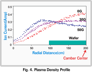
To further reduce capacitive coupling, proprietary Faraday shields are used. Magnetic fields are introduced at the edge of the dielectric tube, which enhances electron trapping. Any desired plasma uniformity is achieved by adjusting magnetic field strength.